Ningbo Volken Technology Co., Ltd. (hereinafter referred to as "Volken") has disclosed its prospectus for initial public offering of shares and listing on the Science and Technology Innovation Board (application draft). Volken is an advanced domestic manufacturer of silicon carbide and boron carbide ceramic materials and products, mastering the complete set of technical processes from material formulation to products for silicon carbide ceramics.
The company has established long-term stable and in-depth business cooperation relationships with leading downstream enterprises. In the field of photovoltaics and semiconductors, customers include Shaanxi Nonferrous Metals, Laplace, GCL Technology, American REC, Northern Huachuang, Songyu Technology, Shanghai Microelectronics, etc; In the field of fluid control, the company's clients include the 14th Research Institute of China Electronics Technology Group, Kaiquan Group, Ningbo Delishi, SPECK Group, and Schlumberger, among others; In the field of aerospace and military industry, the company's clients include the Beijing Space Electromechanical Research Institute.
Volken's predecessor was Fenghua Mechanical Seal Factory and Ningbo Shuanghuan Mechanical Seal Factory, and Mr. Wu Guoping, the old factory director, had been working at the factory as early as 1977.
Now, he is gradually transferring the management rights to his daughter Wu Yanjiao.
However, surprisingly, Volken's IPO is on the Science and Technology Innovation Board, which conflicts with the traditional Ningbo factory director's business operations. What high-tech expertise does this sealing enterprise possess?
1、 From seals for bearings to phased array radar
Industrial upgrading is not only a grand project that benefits the country and the people, but also a very interesting thing from a micro perspective.
There is a company (Wald) that produces diamond cutting tools, but due to fierce competition, it has turned to specialized cutting tools for the consumer electronics industry. As a result, it caught up with the explosion of the panel industry and became a cutting panel tool manufacturer for panel manufacturers such as BOE and Shenzhen Tianma. The company has injected technological content and has also been sought after in the capital market, successfully becoming a listed company on the Science and Technology Innovation Board.
The same is true in the field of seals. Volken's seals are mainly used in industries such as bearings and machinery because of their excellent technology, especially after the introduction of 3D printing technology, the company is able to produce larger and larger seals.
Until one day I made a super large one: a 500mm seal. 500mm, which is 5 meters, is difficult to manufacture with traditional techniques, usually combined with 3D printing and other technologies.
This seal is made of ceramic technology and used on the phased array radar of Chang'e-5.
From the perspective of revenue scale, the company's revenue is only 270 million yuan until 2022. Although technically leading in the field of segmentation, the growth space is very limited.
Especially its proudest technology in fields such as aerospace and military industry accounts for less than 5% of total revenue. This is also related to the particularity of these projects, which are currently not large-scale mass production projects and have limited benefits for the company.
This also gives us a hint from the side that the United States has incubated and grown a large number of high-tech companies such as Boeing, IBM, Qualcomm, etc. through projects such as the lunar landing program. China's aerospace technology must and will inevitably become bigger and stronger, with a long way to go.
2、 Ceramic PCB is an inorganic product that is a suitable material for aerospace equipment.
The thermal conductivity of ceramic substrates is high. For example, the thermal conductivity of aluminum nitride ceramic plates can reach as high as 170~230W/MK. The thermal conductivity of a regular PCB substrate is 1.0W/MK, while the thermal conductivity of a ceramic substrate is that of a regular PCB substrate. About 200 times, the one that needs heat conduction is undoubtedly the long drought sweet dew.
The ceramic substrate itself is an insulating material. Therefore, there is no need for additional insulation materials to manufacture ceramic substrates. In the production of ceramic metallized products, the bonding strength between ceramics and titanium metal can reach 45MPa, and copper metal and ceramics have a better matching coefficient of thermal expansion. Ceramic plates and metal layers can firmly bond under high temperature conditions. Metal wires and ceramic plates may come off.
Although ceramic plates have a brittle texture, they have high mechanical hardness and low dielectric constant, making them suitable for use at high frequencies. If used in the electronic communication industry, the signal loss rate can be significantly reduced.
The ceramic substrate is high-temperature resistant and has a breakdown voltage of up to 2wV. Faced with sudden high voltage, it can ensure the normal operation of the equipment itself and ensure the safety of operators.
Ceramic PCBs have stable chemical properties and can be widely used in electronic products that are corrosive or require long-term immersion, such as automotive LED sensors.
Generally speaking, ceramic metallized products and ordinary PCB products have their own advantages and disadvantages. They will have their own applications in different fields. But with the increase in market demand, the application of ceramic metallized products will become more widespread. As an emerging product, it has excellent performance and is more competitive in the future market.
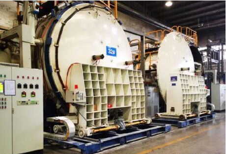
After more than ten years of continuous research and development, Ningbo Volken officially established the Silicon Carbide 3D Printing Business Unit in 2018. It successfully developed 3D printed silicon carbide special ceramic technology with independent intellectual property rights, breaking through a series of key core technologies such as high-performance raw material formula design of silicon carbide special ceramics, industrial grade printing machine design and manufacturing, printing process, controllable sintering of large components, and high-temperature purification, achieving large-scale, ultra-lightweight Intelligent manufacturing of complex structures and high-purity silicon carbide products. The maximum printing size of a single product reaches 2750 mm × 2300 mm × 1000 mm, with advanced structure, excellent performance, high purity, short cycle, low cost, etc.

At present, the company has achieved large-scale production of 3D printed silicon carbide special ceramic products, and various series of high-purity, high-precision, large and complex structural components are widely used in fields such as photovoltaic (granular silicon, single crystal furnace, Topcon), semiconductor (lithography, CMP), and battery (silicon carbon negative electrode). Some of the product performance exceeds similar foreign products, making contributions to the controllable release of core technologies in major industrial fields of the country; In various high-temperature process equipment such as gas deposition, 3D printed silicon carbide high-temperature structural components have successfully achieved upgrading and iteration of traditional products such as C/C and graphite; In the field of aviation and aerospace, the company has achieved efficient and high degree of freedom rapid manufacturing and practical application of ultra lightweight topological structure large caliber single silicon carbide mirrors, effectively supporting the development of national remote sensing satellites and space infrastructure construction, and enhancing China's core competitiveness in the field of remote sensing exploration technology.